Queue Design in SystemVerilog:

Entry is stored into the Queue in a certain order. The order could be as simple as find any first vacant entry or find a next vacant entry from previous allocation or find the last entry that became available recently.

Queues are used in Digital design when the Data from a Stream is needed to be stored into a Structure, manipulated and taken out of Order based on a protocol or events in the Design.

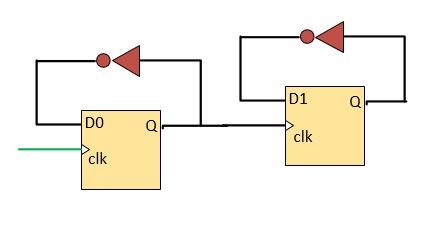
The Entry could be taken out of queue (de-allocated) based on a certain protocol. If the protocol involves series of events that are common for each entry then a FSM shown below is used. However, if each entry in the queue needs a separate event then just a Combinational Trigger logic to clear a valid bit maybe sufficient.

Here’s an example of 8 Entry Queue that uses FSM for each Entry manipulation :

Queue FSM
parameter   DEPTH         = 8;
parameter   INVALID_STATE = 4'b0001;
parameter   VALID_STATE   = 4'b0010;
parameter   EVENT1_STATE  = 4'b0100;
parameter   DISABLE_STATE = 4'b1000;

logic [DEPTH-1:0]      state_ps[3:0];
logic [DEPTH-1:0]      state_ns[3:0];  
logic                  queue_empty;
logic                  queue_full;

logic [DATA_WIDTH-1:0] queue_data[DEPTH-1:0];
logic                  queue_valid[DEPTH-1:0];
logic [DATA_WIDTH-1:0] data_out[DEPTH-1:0];

logic [DEPTH-1:0]      new_entry;
logic [DEPTH-1:0]      allocate_entry;
logic                  allocate_new;

logic [DEPTH-1:0]      event1_started;
logic [DEPTH-1:0]      event1_completed;
logic [DEPTH-1:0]      event1_dis;

genvar x, i, j;

always_comb begin
  casez (state_ps[0])
    8'b????_???1 : new_entry = 8'h1;
    8'b????_??10 : new_entry = 8'h2;
    8'b????_?100 : new_entry = 8'h4;
    8'b????_1000 : new_entry = 8'h8;
    8'b???1_0000 : new_entry = 8'h10;
    8'b??10_0000 : new_entry = 8'h20;
    8'b?100_0000 : new_entry = 8'h40;
    8'b1000_0000 : new_entry = 8'h80;
    default      : new_entry = '0;
  endcase 
end

assign allocate_entry = (~queue_full & allocate_new) ? new_entry : 8'b0;

always_comb begin
  for (int entry = 0; entry < DEPTH; entry++)
    casez (state_ps[entry])
      INVALID_STATE : if(entry_dis[entry])
                        state_ns[entry]   = DISABLE_STATE;
                      else if(allocate_entry[entry])
                         state_ns[entry]  = VALID_STATE;
                       else
                         state_ns[entry]  = INVALID_STATE;
 
     DISABLE_STATE  : if(~entry_dis[entry])
                         state_ns[entry]  = INVALID_STATE;
                      else
                        state_ns[entry]   = DISABLE_STATE;                        

      VALID_STATE   : if(event1_started[entry]) 
                         state_ns[entry]  = EVENT1_STATE;
                      else
                         state_ns[entry]  = VALID_STATE;

      EVENT1_STATE :  if(event1_completed[entry])
                         state_ns[entry] = INVALID_STATE;
                       else
                         state_ns[entry]  = EVENT1_STATE;

      default      :  state_ns[entry] = state_ps[entry]; 
    endcase
  end
end

generate
for (x = 0; x < DEPTH; x++)
  always_ff @(posedge clk or negedge reset) begin
    if(~reset)
      state_ps[x] <= INVALID_STATE;
    else
      state_ps[x] <= state_ns[x];
  end
end
endgenerate

assign event1_started   = request_sent[DEPTH-1:0]; // From other Module
assign event1_completed = response_ack[DEPTH-1:0]; // From other Module
assign entry_dis        = entry_disable[DEPTH-1:0];// From other Module 

//Queue Data maintenance
generate
for (i = 0; i < DEPTH; i++)
  always_ff @(posedge clk or negedge reset)
    if(~reset | event_completed[i]) begin
      queue_data[i]   <= queue_data[i]; // Can be zero if required 
      queue_valid[i]  <= 1'b0;
    end
    else if (allocate_entry[i]) begin
      queue_data[i]   <= data_in;
      queue_valid[i]  <= 1'b1;
    end
    else begin
      queue_data[i]   <= queue_data[i];
      queue_valid[i]  <= queue_valid[i];
    end
  end
 end
endgenerate


//Queue Data readout of multiple entries.
generate
 for (j = 0; j < DEPTH; j++)  
   assign data_out[j] = (event_completed[j] & queue_valid[j]) 
                         ? queue_data[j] :'0; 
 end
endgenerate

Here request & response could be sent and received from another Design Module. These Events (Started and Completed) could happen one per entry per cycle or multiple entries per cycle. Hence, there are multiple entries getting State updates i.e multiple entries taken out of Queue.

If only single event is expected to complete every cycle then Decoder is needed to extract out single Data element out of queue as shown below:

logic [2:0] entry_dec;
always_comb begin
 unique case (event_completed[7:0])
    8'h0000_0001 : entry_dec = 3'h0;
    8'b0000_0010 : entry_dec = 3'h1;
    8'b0000_0100 : entry_dec = 3'h2;
    8'b0000_1000 : entry_dec = 3'h3;
    8'b0001_0000 : entry_dec = 3'h4;
    8'b0010_0000 : entry_dec = 3'h5;
    8'b0100_0000 : entry_dec = 8'h6;
    8'b1000_0000 : entry_dec = 8'h7;
  endcase 
end

//Queue Data readout of Single entry
assign data_out = ((|event_completed) & queue_valid[entry_dec]) 
                   ? queue_data[entry_dec] :'0; 
 

Entry disable is done in order to limit or disable the number of Entries Queue or apply back-pressure on preceding Design module. This programming is usually done via Firmware and used as a effective tool to Test out Corner cases.

Synchronous FIFO :

Fifo (first-in-first-out) are used to for serial transfer of information whenever there is a difference of Transfer rate. The Transfer rate may differ due to difference in number of ports, frequency or data-width between source and destination.

The FIFO width is chosen to compensate for the Transfer rate and is calculated as follows:

Fifo size = Source Freq. * ports * Data-with / Dest. Freq. * ports * Data-with

Ex: Source : Port = 1, Freq. = 100KHz, Data-Width = 20
Destination : Port = 2, Freq. = 50KHz, Data-Width = 10
FIFO Size : 1*100*20/ 1*50*10 = 4 Entries

If the FIFO size is a fractional number then we round-up the FIFO size to nearest largest whole number. For Ex 4.33 -> 5.

Here’s a SV reference for 8 Entry deep FIFO with Data-Width of 32 bits :

8-Entry FIFO
logic [3:0] wraddr, rdaddr;
logic [7:0] wren, rden;
logic [31:0] data_ff[7:0];
logic [31:0] data_in, data_out;
logic wr_en, rd_en;
logic fifo_empty, fifo_full;

always_comb begin
if(!fifo_full & wr_en)
 wraddr = wraddr + 1;
else
 wraddr = wraddr_ff;
end

always_comb begin
 if(!fifo_empty & rd_en)
   rdaddr = rdaddr + 1;
 else
   rdaddr = rdaddr_ff;
end

always_ff @(posedge clk or negedge reset) begin
 if(!reset)
   rdaddr_ff <= 0;
 else if (rd_en)
  rdaddr_ff <=  rdaddr;
 else
  rdaddr_ff <= rdaddr_ff;
end

always_ff @(posedge clk or negedge reset) begin
 if(!reset)
   wraddr_ff <= 0;
 else if (wr_en)
  wraddr_ff <=  wraddr;
 else
  wraddr_ff <= wraddr_ff;
end

assign fifo_full = (wraddr[2:0] == rdaddr[2:0]) & 
                   (wraddr[3] != rdaddr[3]);

assign fifo_empty = (wraddr[2:0] == rdaddr[2:0]) & 
                    (wraddr[3] == rdaddr[3]);

assign wren = (wr_en == 1'b1) ? (1 << wraddr) : 8'b0;
assign rden = (rd_en == 1'b1) ? (1 << rdaddr) : 8'b0;

genvar i;
generate 
for (i = 0; i < 8; i++) begin  
always_ff @(posedge clk or negedge reset) begin
  if(wren[i]) 
     data_ff[i]  <= data_in;
   else
      data_ff[i] <= data_ff[i];
  end
end
endgenerate

always_comb begin
 for (int j = 0; j < 8; j++) begin
  if(rden[j]) 
    data_out = data_ff[j];
  else
    data_out = 8'b0;  
end

If the Fifo Width is not binary multiples of 2 , detecting full and empty conditions is difficult using above method. Alternately, we can use below two implementations that are more scalable with Fifo Widths:

1st implementation can be followed with a use of Single Counter to track Full and Empty conditions :

logic [2:0] fifo_count, fifo_count_ff;

always_comb begin
unique casez ({rd_en, wr_en})
2'b00 : fifo_count = fifo_count_ff;
2'b01 : fifo_count = (fifo_count_ff == 3'b111) ? 3'b111
: (fifo_count_ff + 3'b001);
2'b10 : fifo_count = (fifo_count_ff == 3'b0) ? 3'b0
: (fifo_count_ff - 3'b001);
2'b11 : fifo_count = fifo_count_ff;
endcase
end

always_ff @(posedge clk or negedge reset) begin
if(!reset)
fifo_count_ff <= 3'b0;
else
fifo_count_ff <= fifo_count;
end

assign fifo_full = (fifo_count == 3'b111);
assign fifo_empty = (fifo_count == 3'b0);

2nd implementation is using read and write roll-over pointers on wraddr and rdaddr.

logic wr_rollover, wr_rollover_ff;
logic rd_rollover, rd_rollover_ff;

always_comb begin
if((wraddr == 3'b111) & (wr_en & !rd_en))
wr_rollover = ~wr_rollover_ff;
else
wr_rollover = wr_rollover_ff;
end

always_ff @(posedge clk or negedge reset) begin
if (!reset)
wr_rollover_ff <= 1'b0;
else
wr_rollover_ff <= wr_rollover;
end

always_comb begin
if((rdaddr == 3'b0) & (!wr_en & rd_en))
rd_rollover = ~rd_rollover_ff;
else
rd_rollover = rd_rollover_ff;
end

always_ff @(posedge clk or negedge reset) begin
if (!reset)
rd_rollover_ff <= 1'b0;
else
rd_rollover_ff <= rd_rollover;
end

assign fifo_full = (wraddr[2:0] == rdaddr[2:0]) &
(wr_rollover != rd_rollover);

assign fifo_empty = (wraddr[2:0] == rdaddr[2:0]) &
(wr_rollover == rd_rollover);

CAM (Content-Addressable-Memory):

CAM is a type of memory that enables faster and efficient searching for specific data patterns. It allows search-key as an input & uses the search to pattern-match. The pattern matching can be done on whole row/content of the memory to create match flags. The match logic is combinational logic using comparators.

To design a CAM-based circuit for exact match lookup, you would typically follow these steps:

  1. Determine the size and organization of the CAM: Define the number of entries and the width of each entry based on the requirements of the specific application.
  2. Determine the search key width: Decide on the width of the search key, which is the data pattern you want to match against the entries in the CAM.
  3. Implement the CAM cell: Each CAM cell consists of two components: a data storage element and a comparator. The data storage element holds the entry value, while the comparator compares the search key with the stored value. If there is an exact match, the corresponding match flag is set.
  4. Design the control logic: Implement the control logic to control the read and write operations of the CAM, as well as the search operation.
  5. Connect multiple CAM cells: Connect the CAM cells in parallel so that all entries can be searched simultaneously. Each CAM cell’s match flag will indicate if there is a match or not.
  6. Handle multiple matches: If the CAM is designed to handle multiple matches, additional logic is required to handle scenarios where multiple entries match the search key.
module cam_cell (
  input clk, rst,write_en, read_en,
  input [CAM_WIDTH-1:0] search_key, 
  output [CAM_WIDTH-1:0] cam_out,
  output cam_full, match_found
);
  logic [CAM_WIDTH-1:0] cam_mem [NUM_CELL-1:0]; // Array to store CAM cell data
  logic [NUM_CELL-1:0]  match_flag; // Flags indicating a match for each CAM cell
  logic [NUM_CELL-1:0]  valid, valid_comb; // Valid flags for each CAM cell

  always_ff @(posedge clk or negedge rst) begin
    if (!rst) begin
      match_flag <= '0;
      valid <= '0;
    end
    else begin
      match_flag <= match_flag;
      valid <= valid_comb;
    end   
  end

  always_comb begin
    foreach (int i = 0; i < NUM_CELL; i++) begin
      if (read_en || write_en) begin
        if (search_key == cam_cell[i])
          match_flag[i] = 1'b1; // Set match flag if search key matches CAM cell data
        else
          match_flag[i] = 1'b0; // Reset match flag otherwise
      end
    end
  end

  always_comb begin
    foreach (int i = 0; i < NUM_CELL; i++) begin
      if (match_flag[i] && read_en) 
        cam_output = cam_mem[i]; // Set output to the CAM cell data if a match is found
    end
  end

  generate
    foreach (int i = 0; i < NUM_CELL; i++) begin
      always_ff @(posedge clk or negedge rst) begin
        if ((!cam_full) && write_en && (!match_found) && !(valid[i])) begin
          cam_mem[i] <= search_key; // Write the search key to the CAM cell if entry not found.
          val_comb[i] <= 1'b1;   
        end
      end
    end
  endgenerate

  assign match_found = (|match_flag); // Set match_found output if any match flag is true
  assign cam_full = (&valid); // Set cam_full output if all valid flags are true

endmodule
Summary:
The code represents a module for a Content-Addressable Memory (CAM) cell. It stores data in an array of CAM cells if the match is not found and checks for matches between the input search_key and the data stored in each cell. The module provides outputs indicating if a match is found, if the CAM is full, and the matched data from the CAM cell. It includes sequential and combinational logic to handle the match flags, validity flags, writing to CAM cells, and setting the outputs accordingly.

Content-Addressable Memory (CAM) has its own set of advantages and disadvantages. Here are some pros and cons of CAM memory:

Pros:

  1. High-speed Search: CAM memory enables parallel search operations, allowing for fast and efficient data retrieval. It can search for a specific content or address in a single clock cycle, making it ideal for applications that require quick access to data.
  2. Associative Matching: CAM memory provides associative matching capabilities, allowing it to match input data to stored data without the need for explicit address calculations. This feature is beneficial for applications that involve pattern matching, data filtering, or database queries.
  3. Simplicity of Access: CAM memory simplifies the process of data access by eliminating the need for memory addresses. Instead, the user can directly search for the desired data, resulting in reduced complexity in memory management.

Cons:

  1. Higher Power Consumption: CAM memory typically consumes more power compared to other memory types due to its parallel search and match operations. The power requirements can limit its usage in power-constrained devices or battery-powered systems.
  2. Cost: CAM memory is generally more expensive to manufacture compared to other memory technologies, such as random-access memory (RAM) or read-only memory (ROM). The complexity and additional circuitry required for associative matching contribute to its higher cost.
  3. Limited Density: CAM memory often has a lower density compared to traditional RAM or ROM. The additional circuitry required for associative matching reduces the number of memory cells that can be packed in a given area, limiting the overall storage capacity of CAM memory.
  4. Write Operation Complexity: Writing data to CAM memory can be more complex compared to other memory types. As CAM relies on parallel matching, updating or modifying specific data requires additional circuitry and can be slower compared to simple write operations in RAM.

CAM memory is well-suited for certain applications that demand high-speed search and associative matching, but its higher cost, power consumption, and limited density may make it less suitable for other use cases.

Von-Neumann architecture and Harvard architecture:

Von Neumann architecture and Harvard architecture are two different designs for computer architecture.

In Von Neumann architecture, the CPU and memory share the same bus to access data and instructions. This means that the same path is used for both data and instruction fetching. This design is simpler, but it can lead to slower performance because the CPU and memory are competing for the same resources.

On the other hand, Harvard architecture separates the CPU and memory by using different buses for data and instructions. This means that the CPU and memory do not have to compete for the same resources, leading to faster performance. However, this design is more complex and can be more expensive to implement.

In summary, Von Neumann architecture is simpler but can lead to slower performance, while Harvard architecture can be more complex but can lead to faster performance.

Examples of computers that use Von Neumann architecture include:

  • Most personal computers and laptops, such as those running Windows or macOS operating systems.
  • Most servers, such as those running Linux or Windows Server operating systems.
  • Most smartphones and tablets, such as those running iOS or Android operating systems.

Examples of computers that use Harvard architecture include:

  • Some embedded systems, such as those used in industrial control systems or consumer electronics devices.
  • Some digital signal processors (DSPs) and microcontrollers, such as those used in audio processing or motor control applications.
  • Some supercomputers, such as Cray X1 or Fujitsu VPP5000, these machines have separate buses for instructions and data, which can lead to faster performance.

A diagram of Von Neumann architecture would typically show a single bus connecting the CPU and memory. The CPU would have a single set of instructions for reading and writing data to memory.

Here’s an example of a simplified diagram of Von Neumann architecture:

 +------------+    +------------+
 |            |    |            |
 |   CPU      |<---| Memory     |
 |            |    |            |
 +------------+    +------------+

A diagram of Harvard architecture would typically show two separate buses, one connecting the CPU to memory for instructions and another connecting the CPU to memory for data. The CPU would have separate instructions for reading and writing instructions and data.

And an example of a simplified diagram of Harvard architecture:

 +------------+    +------------+
 |            |    |            |
 |   CPU      |<---| Instruction|
 |            |    |    Memory  |
 +------------+    +------------+
                             |
                             |
                             v
                        +------------+
                        |            |
                        |    Data    |
                        |    Memory  |
                        +------------+

XOR based clock gating & implementation:

Clock gating is way to save power in synchronous logic by temporarily shutting-off clocks in sequential logic. The clock gating logic could be based on functional behavior of sequential logic or could be purely based of detection of Traffic activity through the logic block. More details are specified in clock-gating section here : 

XOR clock gating : In order to understand XOR based clock gating, let us first understand the property of XOR logic. Here X and Y are inputs and Y is output of XOR gate.

X   Y  Output
0   0   0
0   1   1
1   0   1
1   1   0

XOR logic has a property that allows us to detect if 2 inputs are different i.e if 2 inputs are different the output is 1 otherwise its 0. Also, XOR allows the bits to be inverted if the bits are XORed with 1.

In case of XOR clock gating, the information(A) to be stored is inverted using XOR with 1s (Abar), then, the information to be stored is compared with current information(B) in the flops (again using XOR) and if more than 50% of the bits differ in terms of polarity, then the inverted information (Abar) is stored instead of information(A). This reduces number of bit-flips required for storage of information of A into B thereby saving switching power.

For E.g:
Consider a 10-bit Sequential logic (B[9:0]) storing a value on a valid and this value needs to be written and read (bout) every clock cycle.

logic [9:0] A;         // new info to be written
logic [9:0] Ainv;      // Xored info
logic [9:0] Abar;      // inverted info
logic [9:0] B;         // info to be Stored
logic [3:0] Ainv_cnt;  // Inverted count 
logic       save_inv; // Inversion indicator
logic       save_inv_ff; // Inversion indicator
logic       valid;    // incoming valid 
logic [9:0] b_out;     // info to be read out

assign Abar =  A ^ {10{1'b1}};
assign Ainv =  A ^ B;

// Count number of 1s
always_comb begin
  Ainv_cnt = '0;  
  for (int cnt = 0; cnt < 10; cnt++) begin
    Ainv_cnt += Ainv[cnt];
  end
end

// Detect if bit-flips are more than 50%
assign save_inv = (Ainv_cnt > 5) ? 1'b1 : 1'b0;

always_ff (@posdege clk or negedge reset) begin
 if(reset) 
   sav_inv_ff <= 1'b0;
 else
   save_inv_ff <= save_inv; 
end

// Store A or Abar to minimize switching
always_ff (@posdege of clk or negedge reset) begin
  if(reset) 
    b <= 10'b0;
  elsif(save_inv & Valid)
    b <= Abar;
  elsif (~save_inv & Valid)
    b <= A;
  else
    b <= b;
end
  
// On read-out, make sure to read correct stored info.
bout = save_inv_ff ? b ^ {10{1'b1}} : b;


Please note that XOR logic for inversion and adders gates for counting the bits increases the combinational gate count of the logic. Also an extra bit(save_inv_ff) is stored additionally. Therefore, any power savings here comes at a cost of Area increase. This Area increase will increase static power but will reduce dynamic or switching power of Flops. Therefore careful analysis is recommended before using this technique. 

In general, this technique is more suitable for highly correlated data. For E.g Media or Video type workloads.
 

Arbiter & FSM :

Question 1 : How do you combine different states in an FSM?. Is there any benefit in combining States?.

FSM states can be combined if the State transitions from/to the States are same. By combining various FSM States we can save on following things:

1. Design Space for Verification: With fewer states we have lesser State transitions to verify hence Verification is easier and faster.

2. Power: With Lesser States less Flops can be needed saving more power. Specifically when we are using.

3. Area & Complexity : With lesser States complexity of combinational logic to calculate next-state logic is simpler and also lesser gates are needed saving area.

Question 2: Design a Fixed Priority Arbiter and Round-Robin Arbiter?

Fixed Priority Arbiter :
Round-Robin Arbiter :
logic [3:0] req;
logic [3:0] grnt;
logic [3:0] mask;
logic [3:0] mask_comb;
logic [3:0] mask_comb_q;
logic [3:0] last_grnt_ff;


//Round-Robin Arbiter version-1 (Masking based- Same cycle Grant)
always_comb begin
  casez(last_grnt_ff[3:0])
    4'b0001 : mask_comb = 4'b1110;
    4'b0010 : mask_comb = 4'b1100;
    4'b0100 : mask_comb = 4'b1000;
    4'b1000 : mask_comb = 4'b1111;
    default : mask_comb = 4'b1111;
  endcase
end

assign mask_comb_q = (req & mask_comb);

always_comb begin
  casez(mask_comb_q[3:0]) 
    4'b1111 : grnt = 4'b0001;
    4'b1110 : grnt = 4'b0010;
    4'b1100 : grnt = 4'b0100;
    4'b1000 : grnt = 4'b1000;
    default : grnt = 4'b0000;
  endcase
end

always_ff @(posedge clk or negedge rst) begin
 if(!rst)
   last_grnt_ff <= 4'h0;
 else if (|req)
   last_grnt_ff <= grnt;
 else
   last_grnt_ff <= last_grnt_ff;
end

//Round-Robin Arbiter version-2 (FSM based- Next Cycle Grant)
always_ff @(posedge clk or negedge rst) begin
  if(!rst)
    grnt_pstate <= 4'h0;
  else
    grnt_pstate <= grnt_nstate;
end

always_comb begin
  casez (grnt_pstate)
    4'b0000 : begin
               casez(req)
               4'b???1 : grnt_nstate = 4'b0001;
               4'b??10 : grnt_nstate = 4'b0010;
               4'b?100 : grnt_nstate = 4'b0100;
               4'b1000 : grnt_nstate = 4'b1000;
               default : grnt_nstate = 4'b0000;
              endcase
              end
    4'b0001 : begin 
               casez(req)
                4'b??1? : grnt_nstate = 4'b0010;
                4'b?10? : grnt_nstate = 4'b0100;
                4'b100? : grnt_nstate = 4'b1000;
                4'b0001 : grnt_nstate = 4'b0001;
                default : grnt_nstate = 4'b0001;
               endcase 
              end
    4'b0010 : begin 
               casez(req)
               4'b?1?? : grnt_nstate = 4'b0100;
               4'b10?? : grnt_nstate = 4'b1000;
               4'b00?1 : grnt_nstate = 4'b0001;
               4'b0010 : grnt_nstate = 4'b0010;
               default : grnt_nstate = 4'b0010;
               endcase
              end
   4'b0100 : begin
              casez(req)
               4'b1??? : grnt_nstate = 4'b1000;
               4'b0??1 : grnt_nstate = 4'b0001;
               4'b0?10 : grnt_nstate = 4'b0010;
               4'b0100 : grnt_nstate = 4'b0100;
               default : grnt_nstate = 4'b0100;
              endcase
             end
   4'b1000 :  begin
               casez(req)
               4'b???1 : grnt_nstate = 4'b0001;
               4'b??10 : grnt_nstate = 4'b0010;
               4'b?100 : grnt_nstate = 4'b0100;
               4'b1000 : grnt_nstate = 4'b1000;
               default : grnt_nstate = 4'b1000;
              endcase
             end
    default : grnt_nstate = gnrt_pstate;
 endcase
end

//Fixed Priority Arbiter version-1 (Priority Mux)
always_comb begin
  grnt[3:0] = 4'b0;
  for (int i = 0; i < 4; i++) 
    if(req[i] == 1'b1) begin
      grnt[i] = 1'b1;
      break;
    end  
  end
end

//Fixed Priority Arbiter version-2 (Priority Mux- Synthesis Friendly)
always_comb begin
  grnt[3:0] = 4'b0;
  casez(req[3:0])
    4'b???1 : grnt = 4'b0001;
    4'b??10 : grnt = 4'b0010;
    4'b?100 : grnt = 4'b0100;
    4'b1000 : grnt = 4'b1000;
    default : grnt = 4'b0000;
  endcase
end

Question 3: What is advantages of using one-hot encoding for FSM ?

One hot Coding simplifies combinational logic and reduces multi-bit Transitions to 2.

For E.g in below State, in any State Transition, one bit goes 1->0 and other goes from 0->1 in a State change. This also reduces power required by the logic.

State0 : 4'b0001
State1 : 4'b0010
State2 : 4'b0100
State3 : 4'b1000

However, if the number of States are more for E.g =>8 then more logic is required and combinational logic and number of Flops can increase Area and Power & in that case binary or Gray coding is preferred.

In some cases, Synthesis Tool can actually optimize the encoding depending on the Trade-off specified in Tool.

Delay Module & Shift Registers :

Here are some Design problems that I have encountered at some point in my experience as a Designer and had discussions with others on possible solutions. Please note that there can be multiple approaches to solve the same problem so there are no exclusive right answers.

Question 1: How to detect a signal coming into a logic domain whose clocks are off?

Signal Capture
Signal Capture
Solution :  We can use a Set-Reset flop (signal_ff) whose clock is actually the Signal that we are trying to detect(bit_in). The Set pin of the signal is tied to 1 and Reset is tied to the level detection logic (reset) of flop as shown.Please note that the signal is asynchronous in nature and should be used carefully.

logic bit_in;
logic signal_ff;
logic reset;

always_ff (@posedge bit_in) begin
  if (reset)
    signal_ff <= 1'b0;
  else
    signal_ff <= 1'b1;
end

assign reset = bit_in & signal_ff;

Question 2: How to detect quickly and efficiently if all bits in a BUS are a) all 0s, b) all 1s, c) any 0s and d) any 0s?

Solution :All zeros can be detected using below logic:
 a) assign allzeros = ~(|bus[7:0]);
 b) assign allones  = (&bus[7:0]);
 c) assign anyzeros = ~(&bus[7:0]);
 c) assign anyones  = (|bus[7:0]);

Question 3: How to design a FIFO or Buffer without explicitly checking Full & Empty conditions ?

Solution:  
This can be done through credit counting logic. 
1. Basically, the fixed number of credits are allocated to the requestor.
2. The requestor agent sends a request to the receiver FIFO/Buffer, its credit is then deducted from credit-counter. 
3. The credit is then incremented whenever FIFO is read out.
4. This Credit counter logic allows FIFO to never get Full as requestor agent is back-pressured whenever credit is not available.

Question 4: How to capture serial stream of Bits and calculate if its 8-bits are odd or even ?

Solution :
In this case, we can use a 8-bit shift Register and simple XOR logic to check if its bits are Odd. The implementation can done as follows :

logic       valid;
logic       bit_in;
logic [7:0] regin;
logic [7:0] regin_ff;
logic       odd_byte;

//8-bit Shift Register:
always_ff (@posedge clk or negedge rst) begin
  if(~rst) 
    regin_ff <= 8'b0;
  elseif (Valid)
    regin_ff <= regin;
  else
    regin_ff <= regin_ff;
end
assign regin = {regin_ff[6:0] bit_in};

//Odd byte calculation
assign odd_byte = (^regin_ff[7:0]);

Question : How to design a delay Module that has an input valid, data and a parameter that defines how many cycle to delay the data and output valid and data?.

Delay Module
Solution :
  In this case we can use a shift register as discussed above.
  However, key thing to note here is that we don't have to shift data. 
  This can be achieved by :
1. Creating a static ID for each data-packet and shifting the ID instead.
3. The data associated with incoming valid is allocated in any of the empty slots by using Find-First logic and an ID is created.
4. The Valid and ID are then shifted until valid reaches MSB.
5. Whenever MSB Valid is detected, the associated ID is used to index Data. 
6. The data is Muxed out and associated Valid and ID are de-allocated/Invalidated.  

ECC (Error Correction Codes) :

ECC refers to Error Correction Codes. Error happens whenever there is a bit flips & information is read incorrectly. The bit flip can be a single or double bit causing single bit errors or double bit errors. The bit flips can occur because of hard Errors or soft Errors.
The hard errors are due to inherent defects of circuits during manufacturing, Temperature-variance and general Wear and Tear. These issues often cause stuck at faults where bit is permanently stuck at 0 or 1. Soft Errors occur due to gamma rays colliding with bits resulting in bit flips. The temporary bit flips are also caused due to noisy environment where electronic interference is high for E.g if a circuit happens to be close to power supply.

There are 3 key parts to the ECC :

ECC Generation:
ECC generation is basically a process of applying an algorithm to calculate extra bits that would be stored with Data. The algorithm is an XOR logic where each ECC bit is derived from XOR of several bits including few of ECC bits. These bits are stored along with Data into memory or array & then retrieved back for Detection and generation. The number of ECC bits for generation is dependent on size of the data & can be calculated using below formula :

SECDED : 2^n+1: where n+1 = number of ECC bits.
DECTED : 2^n+2: Where n+2 = number of ECC bits.

For E.g :
For 8 Bits of Data with single bit correction and double bit detection (SECDED) we would need 3 ECC bits i.e from 2^(2+1).
For 8 Bits of Data with double bit correction and Triple bit detection (DECTED) we would need 4 ECC bits i.e from 2^(2+2).

ECC Detection:
The detection is basically a method to know whether there was an Error. For detection, at the minimum we should know that whether there was a bit flip i.e polarity change and also in some cases also how many bits were flipped. These are the 2 important parts of information that allows us to make decision whether Error can be corrected.
For detection, ECC bits are re-generated with same XOR formula that was used in generation and then these bits are compared against the original ECC bits retrieved from the Memory/Array. If the XOR result of the original and regenerated ECC bits is not 0, then there is a evidence of Error syndrome & hence Error is detected.
In order to understand how many bits were in Error, an Error Syndrome is used. An Error Syndrome is basically a list of codes that are stored and used as a reference. Whenever Error is detected, XOR result is referenced against these stored Codes. If there is a match then the Error can be corrected otherwise Error cannot be corrected even though it was detected.

ECC Correction:
Correction is a process of restoring the data to its original state. This is done by using Error Syndrome. The Error syndrome is unique per bit and if the XOR result match is found then that particular bit is in Error. For E.g for SECDED protection on 8-bit data with 3 bits of ECC, there will be 11 Error Syndrome Codes for detecting single bit Error on each 11 bit positions. In order to correct that bit, if the syndrome matches then the polarity of that particular bit is flipped i.e from 0 -> 1 or 1-> 0 & original value is restored.
It is also important to note that if the XOR result is not 0 (i.e if Error was detected) but no matching Error Syndrome was found then Error cannot be corrected. This typically happens whenever there are more bit flips than the ECC bits can correct. For E.g if there 2 bit flips in SECDED type of protection on Data.

SystemVerilog Assertions :

Assertions are a useful way to verify the behavior of the design. Assertions can be written whenever we expect certain signal behavior to be True or False. Assertions help designers to protect against bad inputs & also assist in faster Debug. Assertions are critical component in achieving Formal Proof of the Design.

In general Assertions are classified into two categories:
1. Concurrent Assertions
2. Immediate Assertions

1. Immediate Assertions: These type of Assertions check the properties that hold True or False all the time i.e Clock independent. For Ex. :

P1 :  if (req.opcode != reserved)
      $error ("opcode Error seen");
assert property (P1);


P2 : assert property (!Read && !Write);

2. Concurrent Assertions: These type of assertions are clock based and therefore property is checked only @posedge or @negedge of the clock. These Assertions are more popular in most of the Synchronous Designs. For Ex. :

P1: assert property @(posedge clk) disable iff(!rst) (req |=> grant);

sequence s1;
 (valid == 1b1);
endsequence

sequence s2:
  ##[1:3] (data != '0);
endsequence

P2: assert property @(posedge clk) disable iff(!rst) (s1 |-> s2);

Since Assertions cannot be synthesized it is necessary to guard them with `ifdef and `endif. Alternately, Assertions are grouped into a dedicated package and the package is selectively added depending on the type of compilation. However, adding it into a package makes difficult to debug as source code is isolated.

Lets take a look at different examples of Assertion Operators:

1. $fell() : Event fell in between 2 consecutive cycles.
// clk enable is 0 after 1 cycle whenever valid is 0.
P1: assert property @(posedge clk) (~val) |-> ##1 $fell(clk_en);


2. $change() : Event changed in between 2 consecutive cycles.
// FSM State changes between 2 cycles whenever ack is received.
P2: assert property @(posedge clk) (~ack) |-> ##[1:2] $change(state);


3. $stable() : Event is stable in between 2 consecutive cycles.
// counter is stable whenever wren is 0.
P3: assert property @(posedge clk) (~wren) |->  $stable(count);


4. $onehot() : Event is onehot encoded.
// FSM State is onehot encoded
P4: assert property @(posedge clk) $onehot(fsm_state);


5. $onehot0() : Event is at the most onehot or it could be all 0s.
// Mux select is onehot encoded at most or could be 0.
P5: assert property @(posedge clk) $onehot0(mux_sel);


6. $rose() : Event rose in between 2 consecutive cycles.
// Grant is seen after 1 cycle whenever request is asserted.
P6: assert property @(posedge clk) (req) |=> $rose(grant);


7. $past() : Event was True in previous cycle.
// If grant was seen then request was seen previously.
P7: assert property @(posedge clk) (grant) |-> $past(req);


8.  ##N : One Event was followed by another event in N cycles. // see 1 for example.


9. ##[M:N] : One Event was followed by another event in between M to N cycles. // see 2 for example


10. [*N] : Event was repeated for at least N consecutive cycles.  
// whenever stall is asserted ack is low for 3 consecutive cycles
P10: assert property @(posedge clk) (stall) |-> (~ack)[*3];


11. if (cond) prop1 else prop2 : If condition (cond) is satisfied then
Property (prop1) is True otherwise property (prop2) is True.
P11: assert property @(posedge clk) if (fifo_empty) (!read_en) else (read_en);


12. Ev1 |-> Ev2 : Whenever Event (Ev1) is True then Event (Ev2) is also True. // see 1 for example


13. Ev1 |=> Ev2: Whenever Event (Ev1) is True then Event (Ev2) is also True 
starting next cycle. // see 6 for example


14. $isunknown() : Check if Event/Signal is X or Z.
// opcode should not be X or Z.  
P14: assert property @(posedge clk) $isunknown(opcode);


15. $countones() : Count the number of 1s in the Signal/Event.
//For a 3-bit Mux-sel, assert select values should be less than 6
P15 : assert property @(posedge clk) ($countones(mux_sel) < 3'h6);


16. k[*M:N] : Event (k) is expected to be repeated between M and N Cycles
 // Power off should result in valid out to be off in between 3 to 5 cycles.  
 P16: assert property @(posedge clk) (pwr_off) |-> (~valid_out)[*3:5];


17. k[->N] : Match the Nth cycle of the Event (k).
//whenever write val is asserted write is seen at 8th cycle.
P17: assert property @(posedge clk) (in_wr) |-> (~write_valid)[->8];


18. k[->M:N] : Match the event (k) is True from M to N Cycle.
//whenever read val is asserted read is seen between 8 to 10 cycles.
P18: assert property @(posedge clk) (in_rd) |-> (~rd_valid)[->8:10];


19. ##[0:$] or ##[*] : Open-ended, Event is True eventually or 
by end of simulation.
// Arbiter will grant request eventually if no stall and request is high.
P18: assert property @(posedge clk) (req & ~no_stall) |-> ##[1:$] grant;


Sequence is also used as a part of Assertions whenever there are a series of events that need to happen in order for the event to hold False or True. Here’s an example of sequence:

sequence req_active;
   //request is de-asserted and seen to be asserted in between 1 to 3 cycles
  (!req)  ##[1:3] $rose(req); 
endsequence

sequence stall_inactive;
 // Stall signal is held 0 to 3 consecutive cycles and then rose on 4th cycle
 (~stall)[*3] ##1 $rose(stall);
endsequence

// whenever sequence req_active is True then sequence stall_active is True.
assert property @(posedge clk) disable iff (~rst) (req_active |-> stall_active);

Its important to note that Assertions should not be more complex than necessary. If the Assertion is complicated then the conditions can be split into multiple Assertions for simplicity and Debug. Also, Assertions also act as useful way to determine if there is an X-prop issue in the logic. This can be simply checked by adding an assertion on control signals to check whether they are driven to known values i.e !$unknown(sig)

Clock Domain Synchronization :

Clock domain synchronization is required when we have signals crossing logic domains that are running on two different Frequencies that are Asynchronous to each other. The signal from source domain needs to be synchronized to destination domain before it can be used. If the synchronization is not performed then it could result into Metastability of the signal & could result into incorrect sampling of the signal at the receiving flop. The process of synchronization can be broadly categorized into 2 types.

  1. Open loop solution.
  2. Closed loop solution.

Open-loop Solution :
2-D flop synchronizer
: Here the source signal is flopped twice on destination clock before its used by destination logic. The 2 Flops allow signal to settle down and sample it correctly without getting into Metastable State. We may also use 3 stages of D-Flops if needed but 2 D-Flops are sufficient for most of the cases. The general rule is period of destination clock should be 1.5 times of source clock period. Example below shows the 2 D-Flop Synchronizer .

2D flop synchronizer
2 D-FLOP Synchronizer : Courtesy: Clifford E. Cummings- SNUG 2001

Binary to Gray Conversion : If we have Multiple bits or a Signal Bus crossing clock domain then it can be converted into Gray code. Conversion to Gray code allows 1-bit difference between signal updates. This allows Synchronizer to be effective as there is less probability of Metastability. The conversion from Gray to Binary is discussed in Async FIFO post.

Synchronized Load Pulse: Another Open loop solution is to pass a synchronized load pulse to destination domain and then use this synchronized pulse to flop in Data bits as shown.

Synchronized Load Pulse
Synchronized Load Pulse : Courtesy: Clifford E. Cummings- SNUG 2001

Closed-Loop Solution :
Synchronized Load Pulse with Feedback
: In closed loop solution a feedback from destination clock domain is received before sending the next signal from source clock domain. This reduces the chances of Metastability even further as original signal is re-tried if clock synchronization does not happen correctly. The feedback Mechanism is done using a simple FSM and feedback signal from destination domain needs to be clock crossed as well.
Due to Feedback mechanism, this type of solution is slower compared to open-loop but more reliable. It can be used to transfer critical control bits from one clock domain to other. For e.g. FSM States , Mux Selects etc. Here’s an example of closed loop solution using Synchronized load Pulse.

Synchronized Load Pulse with Feedback
Synchronized Load Pulse with Feedback : Courtesy: Clifford E. Cummings- SNUG 2001

Async FIFO: Async FIFOs are used for clock crossing data bits or large group of signal buses. In this type of implementation read and write pointers are converted into gray code first and then clock crossed into opposite clock domain. The depth of the FIFO is determined using clock domain frequency and data width. Please refer to Async FIFO implementation post for more details.
Alternately, if the frequency difference is small and data widths are same then the FIFO depth can be restricted to 1. This type of implementation is called 1-depth 2 Register FIFO. The 2 Registers are needed for clock crossing however depth of 1 is used to indicate Full and Empty Conditions. This type of implementation is shown below:

2 Register 1 depth Async Fifo Synchronizer
2-Register 1-depth FIFO :Courtesy: Clifford E. Cummings- SNUG 2001

In general its recommended to create a single instance of clock crossing module. This common module can be instantiated multiple times if needed throughout the Design.

This post only discusses high-level details of CDC but if you are interested in implementation and more in depth Technical details please refer to this Paper by Clifford E. Cummings.

Clock Divider :

In industry, most of clock division happens either through PLL (Phase-locked-loop) in ASIC and through DCM (Digital-Clock-Manger) in FPGAs.

Once clock is available, its possible to have a simple synchronous clock division through few Combinational Gates and D-Flops. Here are few examples of Clock division of equal Duty cycle. Qout (not shown) is the Output of Right-most Flop :

Divide by 2 Counter :

Divide by 2 Counter
Clock divide by 2
Divide by 2 Counter
always_ff @(posedge clk or negedge reset) begin
  if(reset)
    Q <= 1'b0;
  else
    Q <= D;
end

assign D = ~Q;
assign Qout = Q;

Divide by 1.5 Counter :

Divide by 1.5 Counter
Divide by 11/2
Divide by 1.5 Counter
always_ff @(posedge clk or negedge reset) begin
  if(reset)
    Q0 <= 1'b0;
  else
    Q0 <= D0;
end

assign D0 = ~Q0;

always_ff @(negedge clk or negedge reset) begin
  if(reset)
    Q1 <= 1'b0;
  else
    Q1 <= Q0;
end

assign Qout = Q1 | Q0;

Divide by 3 Counter :

Divide by 3 counter
clock divide by 3
Divide by 3 Counter
always_ff @(posedge clk or negedge reset) begin
  if(reset)
    Q0 <= 1'b0;
   else
    Q0 <= D0;
end

always_ff @(posedge clk or negedge reset) begin
  if(reset)
    Q1 <= 1'b0;
   else
    Q1 <= Q0;
end

always_ff @(negedge clk or negedge reset) begin
  if(reset)
    Q2 <= 1'b0;
   else
    Q2 <=  Q1;
end

assign D0 = ~(Q0 & Q1);
assign Qout = Q1 | Q2;

Divide by 4 Counter :

Divide by 4 Counter
Clock division by 4
Divide by 4 Counter
always_ff @(posedge clk or negedge reset) begin
  if(reset)
    Q0 <= 1'b0;
   else
    Q0 <= D0;
end
assign D0 = ~Q0;

always_ff @(posedge Q0 or negedge reset) begin
  if(reset)
    Q1 <= 1'b0;
   else
    Q1 <= D1;
end

assign D1 = ~Q1;
assign Qout = Q1;

Clock and Power Gating Techniques:

There are mainly two types of Power dissipation in CMOS Transistors.

1. Static Power dissipation :
Static Power dissipation is mainly caused due to leakage of Transistors. The leakage could be from any of the sources such as :

1. Gate Leakage through dielectric.
2. Subthreshold leakage when CMOS is off.
3. Junction leakage from source and drain diffusion.
4. Contention Current in ratioed circuits.

Pstat = (Isub + Igate + Icont + Ijunc) * V
Where, V  = Volatage
       I* = Various leakage Currents 

The static Power dissipation is inherent to the properties of Transistor and therefore its efficiency mainly depends on the type/technology of CMOS Transistor. As the Transistors are shrinking Static Power dissipation is increasing as Leakages are higher at smaller Technology nodes.

2. Dynamic Power dissipation:
Dynamic Power dissipation is caused due switching of Transistor i.e from 1->0 or 0 ->1. Also, it can be caused due to short circuit when both pMOS and nMOS are partially ON for very short time :

Pdyn = Psw + Psc
Where, Psw = Switching Power
       Psc = Short Circuit Power
Psw = a * C * V * V * f. 

Where,a = activity factor, 
      V = voltage,
      C = Capacitance,
      f = Frequency

As short-circuit power is often very small, its ignored in Pdyn calculations. Therefore Pdyn is directly proportional to frequency, Capacitance, activity factor & square of voltage. If we are able to reduce any of these factors dynamic power reduces in proportion.

The Total Power is combination of Static and dynamic Power and can be stated as :

Ptot = Pstat + Pdyn

In order to study understand how each Power dissipating factor can be reduced in Static and Dynamic Power dissipation, please refer to Chapter 5 Power of a book CMOS VLSI Design by Neil Weste & David Harris (Refer to Link below).

In a Front-end RTL design, Static Power and dynamic Power can be saved by efficient Power and clock gating techniques.

Power Gating :
In Power gating technique, the source of power to a logic block is turned-off temporarily whenever there is no logical processing needed or no activity is required. This is often done through a dedicated Power Management Unit inside the Design that provides various clock sources to different parts of the design. However, it should be noted that loss of power (e.g P1 domain) results into loss of data so important information such as FSM States and other important Firmware values should be stored (e.g Pon domain) somewhere so that it could be retrieved whenever Power is back and design block is functional again. This useful information is often shared in Power-retention Registers or a local RAM. These Registers and RAM retain power when rest of the logic is powered-off. There are also levels of depth of Power gating depending on the extent and length of the Time, the logic its supposed to be inactive. A good example would be Sleep vs Hibernate in a PC. Here’s an block diagram that gives an overview of Power Gating.

Power Gating Structural Hierarchy

Clock-gating :
Clock gating is a way reducing dynamic Power dissipation by temporary turning-off clock of the Flops on certain parts of the logic or by turning-off enable on gated Flops. In other words, Flops are turned-on only if there is valid information to be stored or transferred. The accuracy with which these clocks are Turned-off is captured by clock gating efficiency. The examples of these 2 types of mechanisms is shown below:

1) Clock Gating with Free running Clocks :

always_ff @(posedge clk or negedge reset) begin
  if(reset)
     Q <= 1'b0;
  else if (clk_en)
     Q <= D;
end


2) Clock Gating with Gated Clocks

always_latch  begin
 if(~clk) 
    clkg_en = enable;
end
   
assign gated_clk = clk & clkg_en;

always_ff @(posedge gated_clk or negedge reset) begin
  if(reset)
     Q <= 1'b0;
  else 
     Q <= D;
end
1) Flop with Clock Enable
power and clock gating
2) Flop with Gated Clock

As a generic guideline, if there a lot of flops in the logic that use same gating enable then its better to design a gated clock implementation. This 2nd implementation is well suited for data-flops and it also decreases Timing-risk on enable (clk_en) as enable signal does not need to travel to every gated flop. Also this type of implementation is able to provide glitch-free clocking. Backend Tools often convert create gated clocks by combining several flops that use same clock gating enable if clock optimization feature is Turned-on during Synthesis. There are also other Tools like PowerArtist that statically analyze RTL design and identify gated Flops, their efficiencies, overall Power of each block and potential flops that could be gated.
The 1st implementation is used where clock gating logic is much diverse and each or some of the flops need a separate functional clock enable. This type of clock gating is also used to hold or freeze the value of flops as a way to debug or Stall the Logic.
There are also levels in Clock gating similar to Power Gating. The first level of clock gating is called Trunk level level gating wherein clock to a a Top level of the design block could be shut-off. Then there is a Leaf level gating wherein parts of the modules could be gated individually while rest of the submodules are still ON.

Clock gating Structural Hierarchy

Clock & Power-down Overrides :
Power and clock overrides are used to ungate the clocks. There maybe cases where there maybe a functional issue that may cause Flops to be gated incorrectly. If such issues occur late in a Project where the Design is in convergence mode it may cause significant delays as Design needs to be re-synthesized after correction of bug. In order to avoid such delays Powerdown & Clock overrides act as backup feature to workaround the issue. These overrides also provide a way of Testing DFT (Design for Test) by allowing way to Scan the flops. The override mechanism is often enabled through Firmware Programming.

Adders :

Adders are used extensively in Computer arithmetic in addition, Subtraction, multiplication and division. There are is a constant attempt to make Adders faster as faster Arithmetic leads to faster Machine , E,g Faster Graphics . At very basic level Adders are classified as Half Adders and Full Adders:

Half Adder : Its a 1-bit Adder with no Carry-in. Output is 1-bit Sum and a Carry-out. Sum is XOR of inputs and Carry out is AND of inputs & is represented as follows:

Sum   = A ^ B;
Carry = A & B;

Gate and block diagram representation of Half Adder is shown below :

Half Adder
Half Adder
(Courtesy: Creative Commons, Attribution-Share Alike 4.0 International )
Half Adder Block Diagram

Full Adder : Its a 1-bit/multi-bit Adder with carry in from previous Adder. Sum and Carry-out are represented as :

Sum    = A ^ B ^ C;
       = A B C + A' B' C' + A' B C' + A B'C';

Carry  = C (A ^ B) + AB;
       = C ( A B' + A' B) + AB; 
       = A B' C + A' B C + A B;

Gate and block diagram representation of Half Adder is shown below :

Full Adder
Full Adder
(Courtesy : Creative Commons Attribution-Share Alike 4.0 International )
Full Adder
Block Diagram

Multi-bit Adders can be formed by combining HA and FA. In each case, calculation of Carry is the most critical part in terms of Timing. Here’s an example of 2-bit Adder & 4-bit Adder formed using 1 HA and multiple FA:

2-bit Adder
4-Bit Adder (Ripple-Carry)
(Courtesy: Creative Commons Attribution-Share Alike 4.0 International )

In order to optimize carry and make Adders fasters, different flavors of Adders have been introduced:
1. Ripple Carry Adder
2. Cary-Save Adder
3. Look-Ahead Carry Adder

Signal Names in Digital Design :

There are various methods of defining signal names in Digital Design. Naming a signal correctly may seem a trivial & underrated task but its important because it often results in faster debug and increases the overall readability of the Code. Defining an intuitive signal could difficult sometimes due to shortage of time at hand or lack of predictability of number of signals needed in the design. Below are few references that can help Designers in faster and intuitive Signal Naming:

Defining Inter-Block Signals : Here Block represents group of Sub-Modules or Modules enclosed in a Top-level Module or Wrapper. Communication between the Blocks may require clock crossing. For Ex. 2 entities within an IP.

Nomenclature : source_destination_signalname_clkdomain_flopStaging

Example 1: logic gen_recv_req_c1ff 
gen   = generator block. 
recv  = receiver block.
req   = signal name (request).
c1    = Clock Domain (optional if same clock domain)
ff    = Staging i.e arriving from a flop.

Defining Intra-Block Signals : These signals have source and destination within the Block but source could be one Submodule & destination could be in another Module within the block. Therefore we can Skip Block name for such cases:

Nomenclature : module1_module2_signalname_staging

Examples:
 
1. logic [7:0] genagt_arb_data_ff

   genagt =  generator agent (Module 1)
   arb    =  Arbiter (Module 2)
   Data   =  Signal Name
   FF     =  Staging i.e Flopped    

2. logic buff_cntrl_sel_comb
   buff  = Buffer (Submodule 1)
   cntrl = Control (Module 2)
   Sel   = Signal Name
   Comb  = Staging

Defining Internal Module/Submodule Signals : These type of signals do not communicate outside as their source and destination are within the Module. For such type of signals, Block, Module, source & destination names can be skipped as communication is between one combinational logic to another combinational logic or Flop and Vice-Versa . Here are few examples :

Nomenclature  : signalname_staging

Examples 1 :
logic eventsel_qual
eventsel  = Event Select (signal name)
qual      = qualified (staging)

Example 2 :
logic stallcyc_ff
stallcyc = Stall Cycle (Signal name)
ff       = flop (Staging)

It is also important to avoid some signal names that could be misleading or unclear, here are examples of unclear Signal Naming :

1. logic arbvalsff; // Difficult to understand without spaces/underscores in between.

2. logic Arb_Val_Sff;// Difficult to grep for some Editors if upper and lower case signals are mixed, also decreases readability.

3. logic arbiter_value_sclock_flopped; // Too long, becomes unreadable.

4. logic arvl_sff; // Too short, becomes unreadable.

5. logic arb_val_ff2; // Numeric Value at the end can cause problems in some Compilers.

6. logic arb_val_inst // '_inst' could be mistaken for a Module Instance

Clocking Blocks:

Clocking blocks are used to trigger or provide sample events to the DUT. Clocking block captures a protocol & are usually defined in an Interface. In certain instances Clocking block protocol can Trigger an event that happens after certain conditions are met. For E.g Trigger counter after Request or Valid is seen. It can also create certain clocking events that are on different clock and are not readily available or logic that has not been coded yet. Clocking blocks provide a way to add asynchronous triggering events without need of explicit clocks & thus avoiding Race conditions in Program or Testbench.

interface example_i(input logic clk);

logic request, grant, stall;

clocking cb_i (@posedge clk);
  input grant, stall;
  output request ##1 grant;
  property check : (~stall & grant) |=> request;
  endproperty
endclocking

endinterface

program test(example_i interf_i);

Prop_1: assert property (interf_i.cb_i.check);

initial begin
  @(posedge clk)
  dut.request = interf_i.cb_i.request;
end

endprogram

Clocking blocks cannot be defined inside Tasks, Functions or Packages and the Scope of the Clocking Block is Static i.e limited to Interface , Program or Module in which its defined.

Input sampling can be done by using clocking block name itself or by using sample signals inside it to get the desired skew.

clocking legal_bus_read @(posedge clk);
  input negedge bus_avail;
  output request_valid ##2 bus_avail;
endclocking

// In a program or Testbench Module

initial begin
  //Option-1
  @legal_bus_read;

  //Option-2
  wait (legal_bus_read.request_valid == 1);
end

SystemVerilog Interface :

Interface with Modports
Interface

SystemVerilog Interface is a convenient method of communication between 2 design blocks. Interface encapsulates information about signals such ports, clocks, defines, parameters and directionality into a single entity. This entity, then, can be accessed at very low level for e.g Register access or to a very high level for E.g Virtual Interface.

Additionally, we can also define Tasks, Functions inside an Interface along with Assertion and SVA Checks. This encapsulation provides portability to Design that can use same interface to communicate differently depending on the type of use. This is achieved by defining Modports and Clocking blocks inside Interface.

Similarly, same design module may use different Interfaces communicate differently if the two interface have same Task or Functions defined.

Here’s an simple example of an Interface :

interface example_inter;
  logic [7:0] data_load;
  logic [7:0] data_read;
  logic rd_en;
  logic wr_en;
endinterface

module primary(example_inter example_if, input clock, reset);
 logic [7:0] data_storage;

 always_ff @(posedge clock) begin
   if(reset)
     data_storage <= '0;
   else
     data_storage <= example_if.data_load;
 end 

 assign example_if.data_read = example_if.rd_en ? data_storage : '0;  
endmodule


module top;
  logic clock;
  logic reset;
  
   example_inter example_if ();
   primary       primary_if 
 (.example_if(example_if), .clock(clock), .reset(reset));  
   
endmodule

Here’s an example of Interface using Modport :

interface example_inter;
  logic [7:0] data_load;
  logic [7:0] data_read;
  logic rd_en;
  logic wr_en;

 modport generator_m (output rd_en, output wr_en, output data_load);
 modport receiver_m 
 (input rd_en, input wr_en, input data_load, output data_read);  

endinterface

module generator (example_inter.generator_m gen_i);
// generator Module code
...
..
endmodule

module receiver (example_inter.receiver_m rec_i);
// receiver Module Code
...
..
endmodule

module top;
 example_inter inter_inst();
 
 generator gen_inst (.gen_i(inter_inst));
 receiver  rec_inst (.rec_i(inter_inst));
endmodule 

Task inside Interface :

Task defined inside interface can be used by different Modules by defining the Task inside Interface. This method allows same Task to be used by different Modules by providing unique values. For E.g. Below, one Task ‘Timer‘ can be used by different Modules for counting purposes by providing unique values of threshold on interface.

interface example_inter;
 logic [2:0] count_value;
 logic [2:0] threshold;

task timer (input logic [2:0] count_value);
//Counter Code to count till count_value
... 
..
endtask

endinterface

module example_delay (example_inter ifc);
logic [2:0] final_count;
assign final_count = ifc.threshold;

// count till Threshold
ifc.timer(final_count); 

endmodule

Asynchronous FIFO :

Asynchronous FIFO is needed whenever we want to transfer data between design blocks that are in different clock domains. The difference in clock domains makes writing and reading the FIFO tricky.

If appropriate precautions are not taken then we could end up in a scenario where write into FIFO has not yet finished and we are attempting to Read it or Vice-versa. This scenario often causes data loss and Metastability issues.

In order to avoid such scenarios, the reading and writing is done via a synchronizer. The synchronizer ensures that read and write pointers calculations are consistent and data in FIFO is not accidentally overwritten or read twice.

However, with the clock crossing we need to ensure that FIFO full and empty conditions are taking into account the clock crossing cycles. In other words, pessimistic full and empty conditions need to be added.

Here’s an example to 8-deep FIFO with Write in aclk domain and read in bclk domain:

logic [3:0] wraddr, wraddr_gray, rdaddr, rdaddr_gray;
logic [3:0] wraddr_b1ff,wraddr_bff, wraddr_aff;
logic [3:0] rdaddr_a1ff, rdaddr_aff, rdaddr_bff;
logic [7:0] wren, wren_qual, rden, rden_qual;
logic [31:0] data_ff[7:0];
logic [31:0] data_in, data_out;
logic wr_en, rd_en;
logic fifo_empty, fifo_full;

always_comb begin
if(!fifo_full & wr_en)
  wraddr = wraddr_ff + 1;
else
  wraddr = wraddr_aff;
end

always_ff @(posedge aclk or negedge reset) begin
 if(!reset)
   wraddr_aff <= 0;
 else if (wr_en)
   wraddr_aff <=  wraddr;
 else
   wraddr_aff <= wraddr_aff;
end

//---- Convert wraddr to Gray code ----//
assign wraddr_gray = (wraddr >> 1) ^ wraddr;

//----- Clock sync to bclk --------//
always_ff @(posedge bclk or negedge reset) begin
 if(!reset) begin
   wraddr_bff  <= 0;
   wraddr_b1ff <= 0;
 end
 else begin
   wraddr_bff  <= wraddr_gray;
   wraddr_b1ff <= wraddr_bff;
 end
end

always_comb begin
 if(!fifo_empty & rd_en)
   rdaddr = rdaddr_bff + 1;
 else
   rdaddr = rdaddr_bff;
end

always_ff @(posedge bclk or negedge reset) begin
 if(!reset)
   rdaddr_bff <= 0;
 else if (rd_en)
   rdaddr_bff <=  rdaddr;
 else
   rdaddr_bff <= rdaddr_bff;
end

//------ Convert rdaddr to Gray code -------//
assign rdaddr_gray = (rdaddr >> 1) ^ rdaddr;

//------- Clock Sync to aclk ----------//
always_ff @(posedge aclk or negedge reset) begin
 if(!reset) begin
   rdaddr_aff  <= 0;
   rdaddr_a1ff <= 0;
 end
 else begin
   rdaddr_aff  <= rdaddr_gray;
   rdaddr_a1ff <= rdaddr_aff;
 end
end

//------- Data Read and Write ---------//
assign wren_qual = (wr_en & !fifo_full) ? 
                   (1 << wraddr) : 8'b0;
assign rden_qual = (rd_en & !fifo_empty) ? 
                   (1 << rdaddr) : 8'b0;

genvar i;
generate
for (i = 0; i < 8; i++) begin  
always_ff @(posedge aclk or negedge reset) begin
  if(wren_qual[i]) 
     data_ff[i]  <= data_in;
   else
     data_ff[i] <= data_ff[i];
  end
end
endgenerate

always_comb begin
 for (int j = 0; j < 8; j++) begin
  if(rden_qual[j]) 
    data_out = data_ff[j];
  else
    data_out = 8'b0;  
end

//------ Full and Empty Conditions -----------------//
assign fifo_full = 
(wraddr_gray[2:0] == rdaddr_a1ff[2:0]) &&
(wraddr_gray[3:3] != rdaddr_a1ff[3:3]);

assign fifo_empty = 
(wraddr_b1ff[3:0] == rdaddr_gray[3:0]);

Alternately, similar to Synchronous FIFO, we can also use synchronized write and read rollover signals in calculation of full and empty conditions.

Rise & Fall-Edge Signal Detection:

As a Digital Designer, often times it is needed to define an interface to communicate to other Design Modules. This communication is defined by a protocol that may involve detection of Rising or Falling edge of a Signal. For E.g Rising edge of request and Falling edge of Ack. In such cases Edge detection logic can be designed as follows:

Rising Edge Detection :

logic rise_edge_sig_a;
logic level_sig_a;
logic level_sig_a_ff;

always_ff @(posedge clk or negedge reset) begin
  if(!reset)
    level_sig_a_ff <= 1'b0;
  else
    level_sig_a_ff <= level_sig_a;
end

assign rise_edge_sig_a = level_sig_a & (~level_sig_a_ff);
Rising Edge Detection

Falling Edge Detection :

logic fall_edge_sig_b;
logic level_sig_b_ff;
logic level_sig_b;

always_ff @(posedge clk or negedge reset) begin
  if(!reset)
    level_sig_b_ff <= 1'b0;
  else
    level_sig_b_ff <= level_sig_b;
end

assign fall_edge_sig_b = (~level_sig_b) & level_sig_b_ff;
Falling Edge Detection

Please note that if your intention is to use Level Signal information & convert it into corresponding pulses (Level-to-Pulse Converter) then this design is not a good design fit. This is because the design is Edge detection circuit and relies on edge of the source signal. Therefore, Level Signal information may get lost in the conversion from Level to Pulse.

Mux/De-Mux/Case Statements in SystemVerilog :

Multiplexers are used to select a single input from several inputs with the help of Select signal. Muxes form a combinational logic that can be written as follows. The number of bits required of select are calculated as 2^n = number of inputs , where n is number of select bits.

logic [3:0] select;
logic output, input;
always_comb begin
case (select[3:0]) begin
4'b0001 : output = input_1;
4'b0010 : output = input_2;
4'b0100 : output = input_3;
4'b1000 : output = input_4;
default : output = 1'b0;
endcase
end

The above logic can also be coded as using “if else” statement using a always_comb or using an assign statement using “? :” operator. In this case Mux becomes a Priority Encoded as priority of input_1 > input_2 > input_3 > input_4.

always_comb begin
if(select == 4'b0001) output = input_1;
else if (select == 4'b0001) output = input_1;
else if (select == 4'b0010) output = input_2;
else if (select == 4'b0100) output = input_3;
else if (select == 4'b1000) output = input_4;
else output = 1'b0;
end

assign output = (select == 4'b0001) ? input_1 :
(select == 4'b0010) ? input_2 :
(select == 4'b0100) ? input_2 :
(select == 4'b1000) ? input_2 :
1'b0;

If the Muxes are being used to drive Data Bus then its recommended that Selects to be driven from Flops (For E.x FSM ) otherwise the outputs may change continuously if the selects are not stable in that cycle. Also, if the select to the Muxes is not from a Flop its recommended to initialize select signal first as it avoids X-propagation into downstream logic:

always_comb begin
select = 4'b0;
case (select[3:0]) begin
4'b0001 : output = input_1;
4'b0010 : output = input_2;
4'b0100 : output = input_3;
4'b1000 : output = input_4;
default : output = 1'b0;
endcase
end

De-Multiplexers or decoders perform opposite operation to Multiplexers. Here a single input is distributed to many outputs depending on the select. The number is bits in select can be calculated as power of 2 of number of outputs. The decoders are often used in converting packed signals to unpacked signals or per entry enable for Arrays.

logic [1:0]  sel;
logic [3:0] out;

always_comb begin
unique case (sel[1:0]) begin
2'b00 : out = 4'b0001;
2'b01 : out = 4'b0010;
2'b10 : out = 4'b0100;
2'b11 : out = 4'b1000;
endcase
end

Mux and De-Mux design in SV is often done using Case Statements. There are different flavors of case statements and each one is used in different scenarios to achieve different results.

Casex : In this type of case statement bits used in comparison can be selectively ignored if the values of comparison are ‘x’ or ‘z’. casex statements can result in different simulation and synthesis results so one needs to be extra careful will using casex. For E.x : When select[2:0] is 3’bxxx the output in simulation could be 2’b01 while in synthesis output could be 2’b11 because select[2:0] becomes 3’b001 in ‘x’ or ‘z’ conditions.

logic [2:0] select;
logic [1:0] output_a;

always_comb begin
casex (select[2:0])
3'bxx1 : output_a = 2'b01;
3'b01x : output_a = 2'b10;
3'b001 : output_a = 2'b11;
3'b100 : output_a = 2'b00;
default : output_a = 2'b00;
end

Casez : In casez statements, bits with ‘z’ values are ignored or treated as don’t-care. However, the bits with ‘x’ values are used in comparison. The casez statements are very useful in creating a priority logic and are more readable than if-else statements.

logic [2:0] selb;
logic [1:0] output_b;

// Priority of selection [0] > [1] > [2]
always_comb begin
casez (selb[2:0])
3'b??1 : output_b = 2'b01;
3'b?10 : output_b = 2'b10;
3'b100 : output_b = 2'b11;
default : output_b = 2'b00;
end

Synthesis Directives : In some instances depending on the compiler it is allowed to pass on compiler directives such as ‘// synthesis full_case‘ and ‘// synthesis parallel_case‘ with the case statement.

logic [2:0] selb;
logic [1:0] output_b;

// 1) Example of full case
// Priority of selection [0] > [1] > [2]
always_comb begin
casez (selb[2:0]) // synthesis full_case
3'b??1 : output_b = 2'b01;
3'b?10 : output_b = 2'b10;
3'b100 : output_b = 2'b11;
end

In full_case, the user explicitly tells synthesis that we do not care about output when the selb = 2’b00. The Mux in this case infers storage and generates less hardware by not evaluating all the possible selb values.

logic [2:0] selc;
logic input_x, input_y, input_w, output_z;
always_comb begin
case (selc) // synthesis parallel_case
3'b001 : output_z = input_x;
3'b010 : output_z = input_y;
2'b100 : output_z = input_w;
endcase
end

In parallel case, user implies that the selection conditions are mutually exclusive so the synthesis generates limited States. Parallel case is often useful in case of one-hot logic for E.g FSM.

In general compiler directives should be avoided as it may result in different Simulation and Synthesis results.

Basic Gates using Muxes :

  • Inverter/NOT Gate using 2:1 Mux
logic input_x;
logic output_y;
assign ouput_y = input_x ? 1'b0 : 1'b1;
  • AND Gate using 2:1 Mux
logic output_y;
logic input_x;
logic input_w;
assign ouput_y = input_x ? input_w : 1'b0;
  • OR Gate using 2:1 Mux
logic output_y;
logic input_x;
logic input_w;
assign ouput_y = input_x ? 1'b1 : input_w;
  • XOR Gate using 2:1 Mux
logic output_y;
logic input_x;
logic input_w;
assign ouput_y = input_x ? ~input_w : input_w;

Operator usage in SystemVerilog:

  • Assign operator: blocking and used in writing Combinational logic.
Ex : assign a = b; 
  • Arithmetic & Assignment operator : Generally used in combinational loops , generate loops in sequential logic.
Arithmetic Operator types
x = y + z; - Add Operator
x = y - z; - Subtract Operator
x = y / z; - Divide Operator
x = y % z; - Modulo Operator
x = y * z; - Multiply operator

Arithmetic Assignment Operator types
a+=1; i.e, a = a + 1;
a-=1; i.e, a = a - 1;
a/=1; i.e, a = a / 1;
a*=1; i.e, a = a * 1;
a%=4; i.e. a = a % 4;
a*=2; i.e, a = a * a;
  • Reduction Operators: Generally, used in combinational control logic:
    logic [3:0] sel;
logic any_sel_hi;
logic all_sel_hi;
logic sel_parity;

any_sel_hi = |sel; // any_sel_hi = sel[3] | sel[2] | sel[1] | sel[0];
all_sel_hi = &sel; // all_sel_hi = sel[3] & sel[2] & sel[1] & sel[0];
sel_parity = ^sel; // sel_parity = sel[3] ^ sel[2] ^ sel[1] ^ sel[0];

inv_sel_parity = ~^sel;
//inv_sel_parity = ~(sel[3] ^ sel[2] ^ sel[1] ^ sel[0]);

inv_any_sel_hi = ~|sel;
//inv_any_sel_hi = ~(sel[3] | sel[2] | sel[1] | sel[0]);

inv_all_sel_hi = ~&sel;
//inv_all_sel_hi = ~(sel[3] & sel[2] & sel[1] & sel[0];
  • Relational Operators : Used for comparison in combinational logic:
logic a;
logic b;
logic c;

assign c = a > b; // c is high/True if a greater than b
assign c = a < b; // c is high/True if a less than b

assign c = a >= b; // c is high/True if a greater than or equal to b
assign c = a <= b; // c is high/True if a less than or equal to b
  • Shift Operators : Logical Shift & Arithmetic Shift.
logic [2:0] a;
logic signed [2:0] b;
logic c, d, e, f;
assign a = 3'b101;
assign b = 3'b101;

// Logical Shift
assign c = a << 1; // shift c by 1 position to left &
// fill the LSB with Zero and remove MSB,
// i.e c = 3'b010;
assign d = a >> 1; // shift a by 1 position to right &
// fill the MSB with Zero and remove LSB,
// i.e c = 3'b010;

//Arithmetic Shift
assign e = b <<< 1; // shift b by 1 position to left &
// fill the LSB with Zero and retain MSB since
// its a signed datatype, i.e e = 3'b110;
assign f = b >>> 1; // shift b by 1 position to right &
// fill the MSB with signed bit and
// remove LSB, i.e f = 3'b110;

// Note that if b were not a Signed datatype,
// results of arithmetic and logical shift would have been same.
// i.e c = e, d = f;

  • Conditional Operator: Used in combinational logic to create Muxes and/or decoder logic.
logic a, b, c, d;
assign c = b ? a : d; // check if b is true if yes, then c = b else c = d.
  • Concatenation & Replication Operator : Used in joining bits to create Bus, concatenation can be on LHS and RHS of assignments. concatenation is treated as packed vector.
logic [4:0] d;
logic [1:0] b,c;
logic a;
// Concatenation
assign d = {a, b, c};

// Replication
d = {5{a}}; // d = {a,a,a,a,a};

// Concatenation + Replication
d = {b,{3{a}}}; // d = {b[1:0], a, a, a};
d = {1{b,c},a}; // d = {b[1:0],c[1:0],a};
  • Logical Operator : Used in comparison of logical expressions. Mainly used to compare and create boolean results. i.e True or false. Arithmetic operators are used if multiple bits are being manipulated.
logic a, b;
logic [3:0] d;
assign a = 1'b1; assign b = 1'b0;
// Result d = 4'h0 if any of a or b is 0.
if(a && b) d = 4'hf else d = 4'h0;

assign a = 1'b1; assign b = 1'b0;
// Result d = 4'hf if any of a or b is 1.
if(a || b) d = 4'hf else d = 4'h0; // Result d = 4'hf;

  • Wildcard Operator : ‘==?’, ‘!=?’. Here operator ‘?’ acts as a wildcard and matches ‘x’ and ‘z’ values from RHS to any value of corresponding bit on LHS.
logic [1:0] c;
logic [1:0] d;
logic e;

assign c = 2'bxz;
assign d = 2'b11;
assign e = (d ==? c); // Result e = 1'b1, as x and z act as wild cards

assign c = 2'b10;
assign d = 2'b1z;
assign e = (d ==? c); // Result e = 1'b0, as z on LHS is not a wild card.
  • Streaming Operator : Streaming operator ‘<<‘ & ‘>>’ are used to pack or unpack the data in specified order. The packing or unpacking can be done on a matching data-type or by type-casting to a particular data-type that match the Widths. If the packed data consists of 4-State type of variable & 2-State type of variable, the result is inferred as 4-state type.
logic a, b, c, d;
logic [3:0] e;
assign e = (>>{a,b,c,d}); // packs a stream of a,b,c,d
{{>>e}}; // unpacks/generates stream of a,b,c,d
{{<<e}}; // unpacks/generates stream of d,c,b,a
(>>{a,b,c,d}) = e; // unpack d=e[0], c=e[1], b=e[2], a=e[3];